 Silicon is the king of the computing world. Almost all commercial integrated circuits have been based on silicon and, for the most part, on a single basic process called complementary metal oxide (CMOS). But the end of silicon may be in sight. Even industry giant IBM acknowledges that silicon’s days are numbered. But why? And what’s going to replace it? There is a whole raft of new materials and partial replacements for silicon in the offing. But I could have written that very sentence two decades ago—maybe even as far back as 1980. Yet silicon remains dominant.
Let’s take a look at why it’s dominant and what materials may eventually knock silicon (and germanium) out of the hot seat.
Why Silicon?
To understand why we ended up with silicon, we need to go back to the beginning. When physicists John Bardeen, Walter Houser Brattain, and William Shockley came up with the first transistor, the material they used was germanium.
Germanium is an excellent semiconductor: It’s power efficient and can be switched very fast. But in the ensuing decades, germanium was muscled out of the mass semiconductor market because it was easier to obtain high-quality silicon.
Once silicon became dominant, the investment in improving silicon devices has kept it on top. This is not because engineers and managers aren’t aware of the benefits of other materials, but because fabricating an integrated circuit requires an intimate knowledge of how a material (or material combination) will respond to the processes used to make a chip. All that knowledge, 40 years in the making, could be lost by switching materials.
Is the material compatible with CMOS, the dominant manufacturing technology? That’s the first question, and for some, the only question. If the answer isn’t yes, you start at a huge disadvantage.
Why New Materials?
Given these restrictions, why are we even looking for new materials?
The answer: speed and power consumption.
Processing speed depends on many factors, but ultimately the faster a transistor can be switched, the higher the potential speed of a processor. Unfortunately, the power consumed by an integrated circuit scales with speed as well. High speed is inevitably linked to higher power consumption. This has to be compensated for by reducing the operating voltage of the integrated circuit or changing the way switches work.
A good example of how new materials can provide an advantage is found in the difference between different memory formats: dynamic random access memory (DRAM) and resistive random access memory (RRAM).
Your computer and phone are probably equipped with DRAM. Each DRAM chip is essentially a grid of tiny capacitors that are charged to store a one and discharged to store a zero. Unfortunately, capacitors leak, so a one will eventually become a zero. To prevent this, the charge in each capacitor is topped up 15 times per second.
A second problem is that changing a one to a zero (and vice versa) requires charging and discharging a capacitor. It depends on the details of the circuit’s layout, but in general, fast charge/discharge means the chip needs to support high current bursts.
This is the sort of load that typically shortens the life of an integrated circuit. So a compromise is reached. Let’s do it slowly, because access to RAM is slow.
On the other hand, RRAM uses a change in material resistance to signify a one or a zero. This does not require a refresh, and writing does not require high currents.
But it does require that the material changes. Usually, PRAM materials are made of metal oxides (think of rust) that are only partially oxidized. Applying a voltage shifts the oxygen around, creating a highly conductive or highly insulating material — the choice is yours.
The switch between conducting and insulating states can take just a few nanoseconds. The currents to read and write are also very small, so RRAM has the potential to be high speed and low power.
But not all RRAM material choices work with CMOS, so engineers may be forced to compromise performance for ease of fabrication if they want to stay on the CMOS path—or do the unthinkable and abandon CMOS.
The Doping Problem
Then we come to the transistors that make up the heart of any processor. Independently of whether we choose germanium or silicon, some impurities, like boron or phosphorus, must be deliberately added (a process called doping) to tailor the electrical properties. A typical doping level is about one phosphorus atom per 1,000 silicon atoms, for example.
In our smallest feature or part of a transistor, which is about 14 nanometers across, we can expect there to be about 100 phosphorous atoms — a change of 10 or so is no big deal. Once we get to features that are only three nanometers across, there will be only a single phosphorus atom per feature. Or none, or three, depending on the luck of the draw.
And since each feature is relatively well isolated from its surroundings, the electrical properties of each feature will be substantially different. This will make engineering a nightmare. The solution requires materials that don’t require doping.
Let’s take a look at some of the possibilities.
Hairy Chips
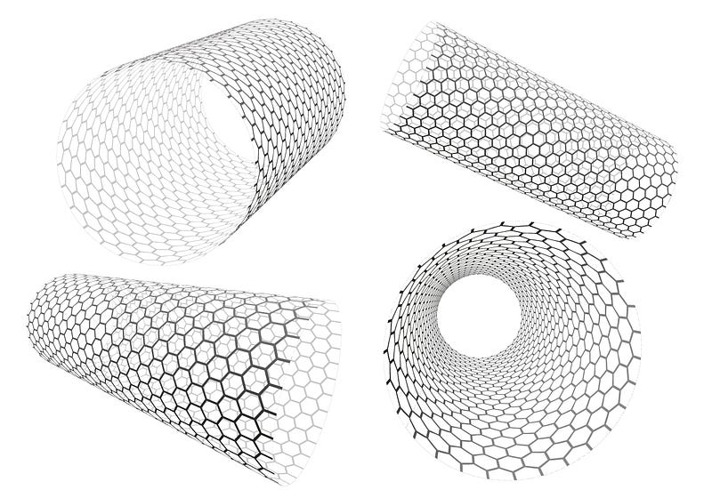
The material routinely touted as the future of computing is the carbon nanotube: a single sheet of carbon atoms, arranged in a hexagonal pattern. The ends of the sheet are pulled up and joined together to create a tube.
Carbon nanotubes are typically less than two nanometers in diameter but can extend for microns in length. This gives them the potential to form lots of different circuit elements.
 Rendering of hexagonal mesh pipe from carbon nanotubes. Photo: Getty
And their progress has been pretty good. In the beginning—way back in the late 1980s—researchers produced uncontrolled tangles of carbon nanotubes with all sorts of diameters (tubes even grew within each other) and mixtures of metallic and semiconductor types. Today, it is almost possible to grow carbon nanotubes to specification.
But growing nanotubes is only half the battle. Researchers quickly demonstrated that fantastic transistors and other electrical elements can be constructed from carbon nanotubes. You just need the patience to individually select and place the nanotube at the right location of a prefabricated circuit. This is the opposite of high-volume manufacturing.
More recently, it has become possible to fabricate circuits based on carbon nanotubes, whose locations are not precisely known. Instead, all that is required is that the tubes are all lined up in the same direction. This allows the surrounding circuitry to be fabricated, knowing that the carbon nanotubes will bridge the electrodes and form a transistor.
That middle step, though—getting the carbon nanotubes onto the right surface—is still not ready for prime time. At present, the state of the art is to grow aligned tubes on one substrate, and then use a kind of high-tech sticky tape to transfer the tubes onto the wafer on which you fabricate your circuit.
I’m not sure if anyone would really consider that ready for high-volume manufacturing. However, if that step can be automated and sped up, then things will be looking up for carbon nanotubes.
Two-Dimensional Carbon
Graphene is another material with promise. It has had even more hype than carbon nanotubes, and for good reason.
First, graphene is a single layer of carbon atoms. Since it is a sheet, you can use lots of preexisting techniques to create circuits in the graphene. Not only that, but graphene is also a pretty good semiconductor and has the potential to have transistor switching speeds that outperform pretty much any other material.
Since it has excellent heat conductivity, you can imagine stacking graphene circuits on top of each other. The heat should flow to the outside edge of the circuit to be sucked away by a cooling circuit. It sounds like a dream material.
 Graphene rendering. Photo: Getty
The reality is less sanguine. All of those excellent properties? They only exist in graphene that is perfect. But we can’t make a perfect graphene sheet that extends over the entire area required for a chip. In fact, we can’t even make an imperfect graphene sheet on top of a wafer for integrated circuits.
No, graphene has to be grown on some other material, like copper, and then carefully released from the copper and transferred to the integrated circuit substrate. Every step in that procedure damages the graphene and makes its properties less desirable. Imagine fabricating a chip but not knowing if there were great big holes in the material you were making it from.
Even worse, because graphene is a single layer, its properties change depending on the material you place it on. The perfect graphene layer has to be encapsulated in some inert material before it can be used.
Then you have the problem of making graphene transistors. Graphene, like silicon, is a semiconductor. Silicon doesn’t conduct until you apply a voltage of about 0.7 volts. Graphene’s equivalent voltage is zero volts. Yes, it’s a semiconductor that behaves just like a metal. So, in designing the graphene circuit, you have to introduce a dopant to increase that voltage.

The New Kid on the Block
That brings me to the final auspicious material: molybdenum disulfide. This is usually styled as another single-layer material, like graphene, but a complete sheet actually consists of a layer of molybdenum sandwiched in layers of sulfur.
As with graphene, creating circuits with molybdenum disulfide through standard fabrication processes is possible. Unlike graphene, molybdenum disulfide behaves a lot more like silicon, so it’s easier to make good transistors. However, it also has many of the better properties of graphene, so those transistors can be fast and power efficient.
Unfortunately, molybdenum disulfide is also like graphene in that it has to be grown on one substrate and then transferred (without damage) to a chip. After which, all the transistors and connections between them are made. Although this can be done, it is not a process that lends itself to the speedy production of microprocessors.
All These Choices: Which One Wins?
What material will provide us with a path beyond silicon?
The new materials we’ve discussed have the right electronic properties to replace silicon and germanium. But the missing step is technical: How to produce integrated circuits in a highly reproducible way—and do it fast and cheap?
In the past, silicon and germanium faced the same problems. It is hard to set up a mature fabrication process. Silicon and germanium integrated circuits created the market and led the industry. As engineers and scientists developed the fabrication process, every improvement was made over an existing process on the same material.
Newcomers have to displace silicon and germanium, which means they cannot begin with low-yield, extremely expensive products. It isn’t good enough to offer a process that beats the previous best with the same material.
Instead, it has to beat the current process on silicon, which makes the barrier to entry very high. Expect a long lead time before any of these materials turn up in your home computer.
No comments:
Post a Comment