


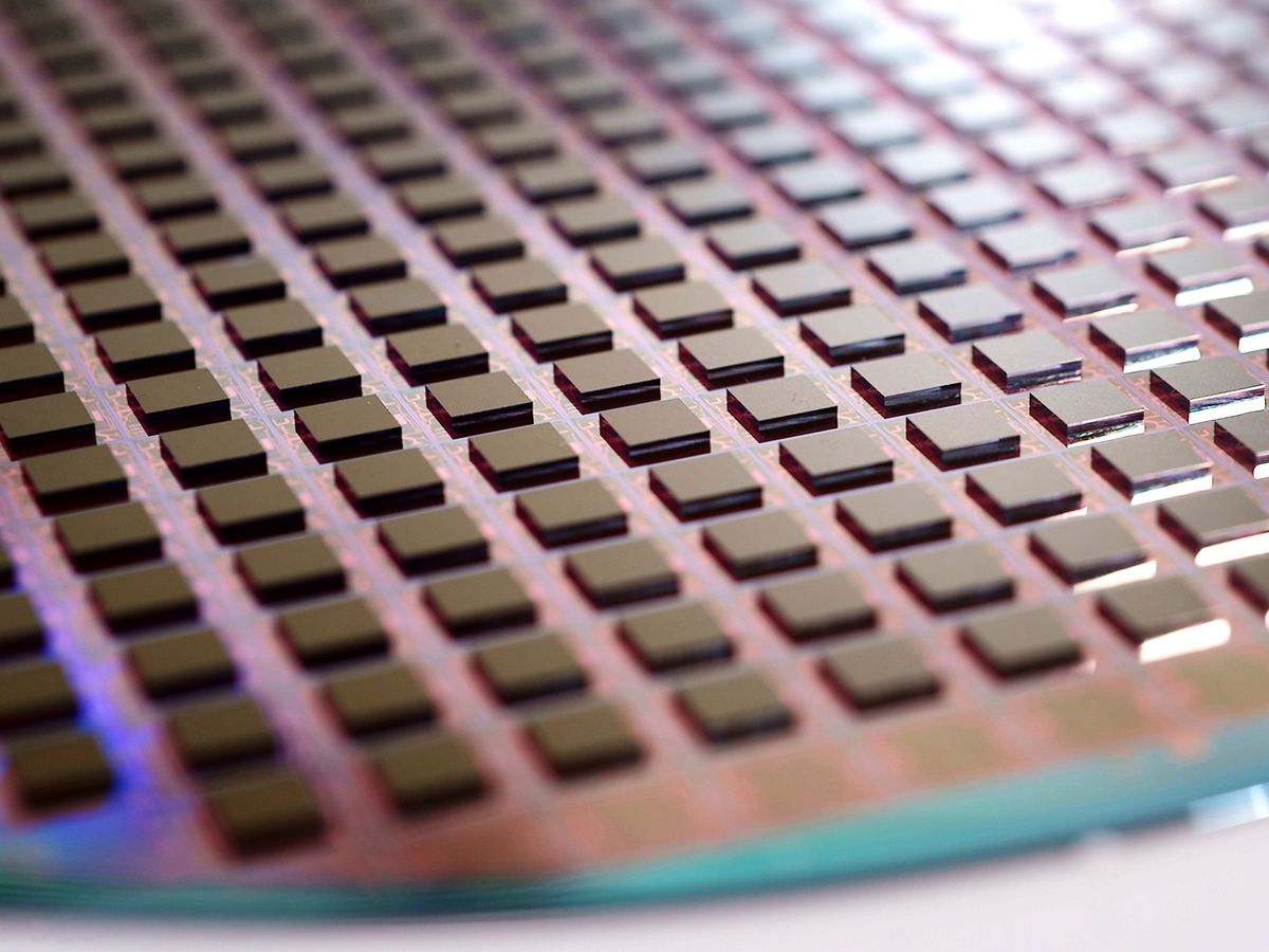
SAMUEL K. MOORE
There was a time, decades really, when all it took to make a better computer chip were smaller transistors and narrower interconnects. That time’s long gone now, and although transistors will continue to get a bit smaller, simply making them so is no longer the point. The only way to keep up the exponential pace of computing now is a scheme called system technology co-optimization, or STCO, argued researchers at ITF World 2023 last week in Antwerp, Belgium. It’s the ability to break chips up into their functional components, use the optimal transistor and interconnect technology for each function, and stitch them back together to create a lower-power, better-functioning whole.
“This leads us to a new paradigm for CMOS,” says Imec R&D manager Marie Garcia Bardon. CMOS 2.0, as the Belgium-based nanotech research organization is calling it, is a complicated vision. But it may be the most practical way forward, and parts of it are already evident in today’s most advanced chips.
How we got here
In a sense, the semiconductor industry was spoiled by the decades prior to about 2005, says Julien Ryckaert, R&D vice president at Imec. During that time, chemists and device physicists were able to regularly produce a smaller, lower-power, faster transistor that could be used for every function on a chip and that would lead to a steady increase in computing capability. But the wheels began to come off that scheme not long thereafter. Device specialists could come up with excellent new transistors, but those transistors weren’t making better, smaller circuits, such as the SRAM memory and standard logic cells that make up the bulk of CPUs. In response, chipmakers began to break down the barriers between standard cell design and transistor development. Called design technology co-optimization, or DTCO, the new scheme led to devices designed specifically to make better standard cells and memory.
But DTCO isn’t enough to keep computing going. The limits of physics and economic realities conspired to put barriers in the path to progressing with a one-size-fits-all transistor. For example, physical limits have prevented CMOS operating voltages from decreasing below about 0.7 volts, slowing down progress in power consumption, explains Anabela Veloso, principal engineer at Imec. Moving to multicore processors helped ameliorate that issue for a time. Meanwhile, input-output limits meant it became more and more necessary to integrate the functions of multiple chips onto the processor. So in addition to a system-on-chip (SoC) having multiple instances of processor cores, they also integrate network, memory, and often specialized signal-processing cores. Not only do these cores and functions have different power and other needs, they also can’t be made smaller at the same rate. Even the CPU’s cache memory, SRAM, isn’t scaling down as quickly as the processor’s logic.
System technology co-optimization
Getting things unstuck is as much a philosophical shift as a collection of technologies. According to Ryckaert, STCO means looking at a system-on-chip as a collection of functions, such as power supply, I/O, and cache memory. “When you start reasoning about functions, you realize that an SoC is not this homogeneous system, just transistors and interconnect,” he says. “It is functions, which are optimized for different purposes.”
Ideally, you could build each function using the process technology best suited to it. In practice, that mostly means building each on its own sliver of silicon, or chiplet. Then you would bind those together using technology, such as advanced 3D stacking, so that all the functions act as if they were on the same piece of silicon.
Examples of this thinking are already present in advanced processors and AI accelerators. Intel’s high-performance computing accelerator Ponte Vecchio (now called Intel Data Center GPU Max) is made up of 47 chiplets built using two different processes, each from both Intel and Taiwan Semiconductor Manufacturing Co. AMD already uses different technologies for the I/O chiplet and compute chiplets in its CPUs, and it recently began separating out SRAM for the compute chiplet’s high-level cache memory.
Imec’s road map to CMOS 2.0 goes even further. The plan requires continuing to shrink transistors, moving power and possibly clock signals beneath a CPU’s silicon, and ever-tighter 3D-chip integration. “We can use those technologies to recognize the different functions, to disintegrate the SoC, and reintegrate it to be very efficient,” says Ryckaert.
 Transistors will change form over the coming decade, but so will the metal that connects them. Ultimately, transistors could be stacked-up devices made of 2D semiconductors instead of silicon. Power delivery and other infrastructure could be layered beneath the transistors.IMEC
Continued transistor scaling
Major chipmakers are already transitioning from the FinFET transistors that powered the last decade of computers and smartphones to a new architecture, nanosheet transistors [see “The Nanosheet Transistor Is the Next (and Maybe Last) Step in Moore’s Law”]. Ultimately, two nanosheet transistors will be built atop each other to form the complementary FET, or CFET, which Velloso says “represents the ultimate in CMOS scaling” [see “3D-Stacked CMOS Takes Moore’s Law to New Heights”].
As these devices scale down and change shape, one of the main goals is to drive down the size of standard logic cells. That is typically measured in “track height”—basically, the number of metal interconnect lines that can fit within the cell. Advanced FinFETs and early nanosheet devices are six-track cells. Moving to five tracks may require an interstitial design called a forksheet, which squeezes devices together more closely without necessarily making them smaller. CFETs will then reduce cells to four tracks or possibly fewer.
 Leading-edge transistors are already transitioning from the fin field-effect transistor (FinFET) architecture to nanosheets. The ultimate goal is to stack two devices atop each other in a CFET configuration. The forksheet may be an intermediary step on the way.IMEC
According to Imec, chipmakers will be able to produce the finer features needed for this progression using ASML’s next generation of extreme-ultraviolet lithography. That tech, called high-numerical-aperture EUV, is under construction at ASML now, and Imec is next in line for delivery. Increasing numerical aperture, an optics term related to the range of angles over which a system can gather light, leads to more precise images.
Backside power-delivery networks
The basic idea in backside power-delivery networks is to remove all the interconnects that send power—as opposed to data signals—from above the silicon surface and place them below it. This should allow for less power loss, because the power delivering interconnects can be larger and less resistant. It also frees up room above the transistor layer for signal-carrying interconnects, possibly leading to more compact designs [see “Next-Gen Chips Will Be Powered From Below”].
In the future, even more could be moved to the backside of the silicon. For example, so-called global interconnects—those that span (relatively) great distances to carry clock and other signals—could go beneath the silicon. Or engineers could add active power-delivery devices, such as electrostatic discharge safety diodes.
3D integration
There are several ways to do 3D integration, but the most advanced today are wafer-to-wafer and die-to-wafer hybrid bonding [see “3 Ways 3D Chip Tech Is Upending Computing”]. These two provide the highest density of interconnections between two silicon dies. But this method requires that the two dies are designed together, so their functions and interconnect points align, allowing them to act as a single chip, says Anne Jourdain, principal member of the technical staff. Imec R&D is on track to be able to produce millions of 3D connections per square millimeter in the near future.
Getting to CMOS 2.0
CMOS 2.0 would take disaggregation and heterogeneous integration to the extreme. Depending on which technologies make sense for the particular applications, it could result in a 3D system that incorporates layers of embedded memory, I/O and power infrastructure, high-density logic, high drive-current logic, and huge amounts of cache memory.
Getting to that point will take not just technology development but also the tools and training to discern which technologies would actually improve a system. As Bardon points out, smartphones, servers, machine-learning accelerators, and augmented- and virtual-reality systems all have very different requirements and constraints. What makes sense for one might be a dead end for the other.
No comments:
Post a Comment